
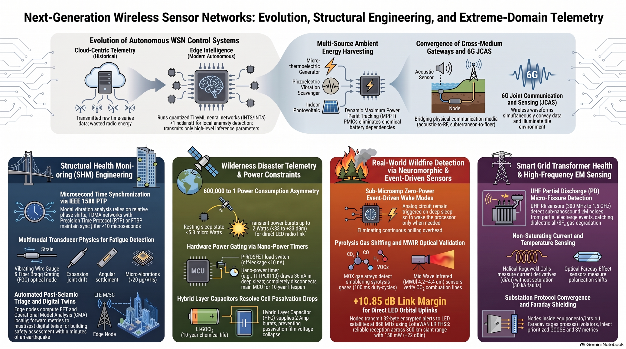
Standard Design Specification: Autonomous Wireless Sensor Network (WSN) Deployment in High-Voltage Utility Environments
- Environmental & Electromagnetic Operational Profile
Deploying autonomous Wireless Sensor Networks (WSNs) across high-voltage (HV), extra-high-voltage (EHV), and ultra-high-voltage (UHV) utility assets—ranging from 69\text{ kV} to 765\text{ kV}+—requires operating in an exceptionally hostile electromagnetic compatibility (EMC) environment. Sensor nodes deployed in these sectors operate in immediate physical proximity to energized conductors carrying thousands of amperes, surrounded by continuous electrostatic and magnetostatic fields, intense corona discharge, and high-energy transient switching surges. Establishing continuous, quantified electromagnetic field baselines is a mandatory engineering prerequisite for designing sensor architectures capable of achieving 10\text{ to }20\text{ year} maintenance-free operational lifespans without experiencing microcontroller logic lock-up, transceiver saturation, or catastrophic dielectric breakdown.
1.1 Quasi-Static Field Densities & Coupling Mechanics
Sensor nodes deployed within electrical utility infrastructure occupy two primary topological positions: line-mounted floating potential nodes (“bird-on-a-wire” topology clamped directly to phase conductors) and substation nodes installed on structural steel framework at earth ground potential. Each topology experiences distinct quasi-static field stress dynamics at fundamental power line frequencies (50/60\text{ Hz}):
- Quasi-Static Electric Fields (E): On overhead transmission conductors, the electric field gradient at the surface of a cylindrical conductor with radius r situated at a distance D above a ground reference plane is defined as: E = \frac{V}{r \ln\left(\frac{D}{r}\right)} Where V represents the line-to-ground operating voltage. On EHV/UHV conductors, surface electric field gradients routinely approach or exceed the dielectric breakdown threshold of ambient air (E_0 \approx 30\text{ kV/cm} or 3.0\text{ MV/m} in dry air), driving localized surface field stresses between 100\text{ kV/m} and 500\text{ kV/m}. This localized electric field drives continuous capacitive displacement currents through any conductive body suspended within the space.
- Quasi-Static Magnetic Fields (B): Governed by Ampère’s Law (\oint \mathbf{B} \cdot d\boldsymbol{\ell} = \mu_0 I), the magnetic flux density B surrounding a conductor core carrying a primary nominal current I at a radial distance r is derived as: B = \frac{\mu_0 I}{2 \pi r} Under nominal operating conditions (1,000\text{ A} continuous line current at a 5\text{ cm} radius from the conductor center), the continuous magnetic flux density reaches approximately 4.0\text{ mT}. During symmetrical system short-circuit faults (I_{\text{fault}} = 20\text{ kA}\text{ to }40\text{ kA}), this flux density spikes to values between 80\text{ mT} and 160\text{ mT} within a quarter-cycle.
Operational Parameter / Stress Factor Line-Mounted (“Bird-on-a-Wire”) Topology Ground-Mounted Substation Topology
Operating Voltage Potential Floating at line potential (69\text{ kV}\text{ to }765\text{ kV}{\text{RMS}}) Fixed at Earth Ground (0\text{ V} potential)
Surface Electric Field Gradient (E) Extreme localized intensity (100\text{ kV/m}\text{ to }500\text{ kV/m}) Low to Moderate (1\text{ kV/m}\text{ to }20\text{ kV/m})
Displacement Current Coupling Mechanism High capacitive coupling to free space / ground plane Stray capacitive coupling to adjacent overhead buses
Nominal Magnetic Flux Density (B) Continuous 4.0\text{ mT} at 1,000\text{ A} (5\text{ cm} radius) Distant 0.01\text{ mT}\text{ to }0.5\text{ mT} spatial gradient
Fault-Current Magnetic Transient Extreme peak surge (80\text{ mT}\text{ to }160\text{ mT} at 20\text{–}40\text{ kA}) Moderate transient induction based on bus proximity
Primary Physical Threat Transient differential voltage (V{\text{diff}}) across chassis Steep ground potential rise (GPR) and common-mode surges
1.2 High-Energy Transient & RF Interference Characterization
Internal sensor microelectronics operating at low logic supply voltages (1.8\text{ V}\text{ to }3.3\text{ V}) are exposed to three distinct high-energy transient regimes alongside continuous radio-frequency interference (RFI):
- Lightning Impulses (LI): Standardized by IEC 60060-1 as a 1.2/50\ \mu\text{s} impulse wave (voltage rising to peak in 1.2\ \mu\text{s} and decaying to half-peak in 50\ \mu\text{s}). Direct strikes or nearby lightning discharges inject transient current pulses ranging from 10\text{ kA} to 100\text{ kA}, inducing severe electromagnetic pulses (EMP) and steep localized ground potential rises.
- Switching Impulses (SI): Originating from circuit breaker operations or capacitor bank switching, these present 250/2500\ \mu\text{s} impulse profiles. While exhibiting lower peak voltage amplitudes than lightning impulses, switching surges deliver sustained energy discharges capable of thermally destroying unhardened transient voltage suppression (TVS) arrays.
- Very Fast Transients (VFTs): Prevalent in Gas-Insulated Switchgear (GIS) when disconnector switches strike restrike arcs across sulfur hexafluoride (\text{SF}_6) gaps. VFTs feature sub-nanosecond to nanosecond risetimes (<3\text{–}5\text{ ns}), voltage slew rates (dV/dt) exceeding 100\text{ kV}/\mu\text{s}, and high-frequency ringing exceeding 100\text{ MHz}. These transients readily couple through intra-winding parasitic capacitances of isolation barriers.
Continuous baseline interference is driven by corona discharge. When localized surface electric field gradients exceed the ionization threshold of air (calculated via Peek’s Law), ambient air ionizes and generates corona discharge pulses with sub-nanosecond risetimes. Corona discharge emits broadband electromagnetic radiation spanning from 100\text{ kHz} to well over 1\text{ GHz}. Unmitigated corona noise raises the ambient RF noise floor, blinding low-noise amplifiers (LNAs) and causing severe packet loss in onboard 2.4\text{ GHz} (IEEE 802.15.4, BLE) and Sub-GHz (Wi-SUN, LoRa) transceivers.
Quantifying these intense environmental field stresses dictates the physical enclosure shielding architecture required to guarantee node survivability.
- Electromagnetic Compatibility (EMC) & Enclosure Shielding Architecture
The physical enclosure serves as the primary line of defense for autonomous sensor nodes, mitigating destructive transient differential potentials, blocking intense broadband RF noise, and preventing physical degradation in high-voltage utility deployments.
2.1 Equipotential Shell Engineering & Faraday Cage Topologies
For line-mounted “bird-on-a-wire” installations, the sensor node operates directly on an energized phase conductor at elevated potentials (e.g., 400\text{ kV}_{\text{RMS}} to ground). The enclosure must form a floating Faraday cage that maintains the internal circuit reference firmly at the phase conductor potential.
During high-frequency transient events, high-voltage traveling waves propagate along the transmission line. If the sensor body exhibits structural inductance or stray capacitance to free space, a destructive dynamic potential gradient develops across the sensor chassis:
V_{\text{diff}} = L_{\text{body}} \frac{di}{dt} + \Delta V_{\text{capacitive}}
A steep traveling wave with a rate of current change (di/dt) of 10\text{ kA}/\mu\text{s} propagating across a structural inductance (L_{\text{body}}) of just 10\text{ nH} produces an instantaneous differential voltage gradient of 100\text{ V} across internal chassis reference points, which can destroy unshielded silicon interfaces.
To analyze total Enclosure Shielding Effectiveness (SE_{\text{dB}}), the engineering design shall model the combined contribution of absorption loss (A_{\text{dB}}), reflection loss (R_{\text{dB}}), and internal multiple-reflection re-reflection correction factors (B_{\text{dB}}):
SE_{\text{dB}} = A_{\text{dB}} + R_{\text{dB}} + B_{\text{dB}}
Electromagnetic absorption loss (A_{\text{dB}}) is directly governed by material wall thickness (t) and skin depth (\delta):
A_{\text{dB}} \approx 8.686 \cdot \frac{t}{\delta} = 8.686 \cdot t \sqrt{\pi f \mu \sigma}
\delta = \frac{1}{\sqrt{\pi f \mu \sigma}}
Enclosures shall be constructed from high-conductivity cast aluminum alloys (such as A356 or Alodine-finished 6061-T6), providing bulk electrical conductivity \sigma \approx 3.8 \times 10^7\text{ S/m}. For 6061-T6 aluminum, the skin depth calculates to \delta \approx 10.7\text{ mm} at 60\text{ Hz}, \delta \approx 82\ \mu\text{m} at 1\text{ MHz}, and \delta \approx 8.2\ \mu\text{m} at 100\text{ MHz} (VFT spectrum). The engineering design shall mandate a minimum outer enclosure wall thickness of t \ge 3\text{ mm}, guaranteeing an absorption shielding effectiveness exceeding >100\text{ dB} across high-frequency transient and corona noise bands.
+——————————————————————–+
| Multi-Layer Shielding & Isolation Architecture |
| |
| Outer Equipotential Enclosure (Cast Aluminum A356 / 6061-T6) |
| Wall Thickness t >= 3 mm |
| +————————————————————+ |
| | Rounded Corona Geometry (Edge Radius R_edge > 15–20 mm) | |
| | Waveguide-Below-Cutoff Penetrations (Aspect l/d >= 3) | |
| | | |
| | Inner Low-Frequency Magnetic Shield: High-Mu Metal | |
| | +——————————————————+ | |
| | | Multi-Layer PCB Ground Plane Architecture | | |
| | | – SiO2 Isolators (CMTI >= 150–200 kV/us) | | |
| | | – 3-Stage Clamping: GDT -> Decoupling -> TVS Array | | |
| | +——————————————————+ | |
| +————————————————————+ |
+——————————————————————–+
2.2 Low-Frequency Magnetic Shielding & Geometry Specifications
Because aluminum exhibits a relative magnetic permeability of \mu_r \approx 1, low-frequency 50/60\text{ Hz} magnetic fields pass unattenuated through standard aluminum walls (\delta \approx 10.7\text{ mm} at 60\text{ Hz}). These magnetic fields induce eddy currents within internal printed circuit board (PCB) loops, inducing noise voltages that cause analog-to-digital converter (ADC) baseline drift.
To protect sensitive analog front-ends (AFEs) and precision ADCs, the design shall mandate a secondary inner magnetic shield shell constructed from high-permeability Mu-metal (nickel-iron alloy, relative permeability \mu_r \approx 50,000\text{–}100,000, saturation flux density B_{\text{sat}} \approx 0.7\text{–}0.8\text{ T}) or grain-oriented silicon steel surrounding the signal-conditioning stage. To prevent Mu-metal saturation during high-current line faults, a multi-layer composite shield topology must be deployed: an outer aluminum layer reflects high-frequency RF, an engineered internal air gap decouples thermal/mechanical stress, and an inner Mu-metal shell shunts low-frequency magnetic flux away from sensitive electronics.
External chassis geometry shall maintain smooth, rounded outer contours. All external edges, seams, structural clamps, and screw recesses shall maintain a minimum edge radius of curvature:
R_{\text{edge}} > 15\text{–}20\text{ mm}
Sharp corners concentrate electric fields, lowering the local breakdown threshold and inducing continuous corona discharge. Maintaining R_{\text{edge}} > 15\text{–}20\text{ mm} prevents local air ionization, eliminating physical enclosure erosion from ozone and preventing localized RFI generation.
2.3 Aperture Mitigation via Waveguide-Below-Cutoff (WBC) & External Antenna Hardening
Environmental sensor ports, solar vents, and mechanical seams represent electromagnetic apertures. Unmitigated apertures permit high-frequency transient fields to enter the enclosure. All non-metallic enclosure penetrations shall implement Waveguide-Below-Cutoff (WBC) physical design rules.
A circular metallic tube penetration with internal diameter d and length \ell acts as a high-pass filter. Starting from the fundamental TE_{11} mode wave equation for a circular waveguide:
f_c = \frac{1.841 \cdot c}{2\pi r} = \frac{1.841 \cdot c}{\pi d}
Substituting c \approx 3 \times 10^8\text{ m/s} yields the simplified numerical expression for cutoff frequency (f_c):
f_c \approx \frac{175.7}{d\text{ (mm)}}\text{ GHz}
For frequencies below f_c, electromagnetic waves decay exponentially along the tube length. The total attenuation (\alpha_{\text{dB}}) is defined by:
\alpha_{\text{dB}} \approx 27.3 \cdot \frac{\ell}{d}
To guarantee >80\text{ dB} of attenuation across transient frequencies up to 10\text{ GHz}, aperture dimensions shall satisfy d \ll \frac{c}{10 f_{\text{transient}}} while enforcing a physical aspect ratio of \ell/d \ge 3.
Antennas cannot be enclosed within a continuous metal Faraday shield and must sit externally. The external RF interface shall feature a coaxial bulkhead connector with a multi-stage isolation architecture:
External Antenna Input
│
[C_iso] (HV Series Ceramic Capacitor, > 3 kV Rating)
│
├───────[ GDT ]───────┐ (Gas Discharge Tube: Primary Surge > 10 kA)
│ │
├───────[ TVS ]───────┤ (Bidirectional TVS Array: Fast Clamping < 1 ps)
│ │
To LNA / RF Transceiver [Chassis Ground Shield]
The center conductor shall incorporate high-voltage series ceramic isolation capacitors (C_{\text{iso}}, rated >3\text{ kV} dielectric withstand) to block low-frequency common-mode surges, backed by parallel Gas Discharge Tubes (GDTs) and fast-acting bidirectional TVS arrays shunting directly to the outer aluminum chassis.
Physical enclosure shielding provides the outer protective envelope, requiring complementary internal PCB-level hardening to prevent logic corruption.
- Internal Circuit Hardening & Galvanic Isolation Requirements
High-frequency transients that breach physical shielding or propagate through external interface cabling can induce logic latch-up, memory corruption, or permanent dielectric destruction within internal CMOS microcontrollers. Printed circuit board layout and component selection shall follow strict high-frequency EMC design principles.
3.1 PCB Layout & Loop Minimization
The primary source of transient susceptibility on circuit assemblies is inductive loop coupling. High rate-of-change magnetic fields (dB/dt) induce transient voltages (V_{\text{induced}}) within closed PCB trace loops in accordance with Faraday’s Law:
V_{\text{induced}} = -\frac{d}{dt} \iint \mathbf{B} \cdot d\mathbf{A}
To eliminate inductive loop area (A), all multi-layer PCBs shall incorporate continuous, un-cut ground reference planes directly adjacent to every signal routing layer. Differential signal pairs (such as RS-485, SPI, or high-speed sensor buses) shall be tightly routed on adjacent layers directly over solid reference planes without underlying slots or plane split cutouts. Ground plane cutouts increase the return path loop area, causing severe high-frequency voltage induction during transient events.
3.2 Galvanic Isolation & Common-Mode Transient Immunity (CMTI)
Galvanic isolation barriers are required between high-voltage sensing transducers and low-voltage digital processing cores. Standard optocouplers are strictly forbidden in utility-grade designs. Standard optocouplers feature large parasitic inter-electrode capacitance (C_{\text{parasitic}} \approx 0.5\text{–}2\text{ pF}). During steep 100\text{ kV}/\mu\text{s} VFT transients, this parasitic capacitance drives destructive high-frequency displacement currents (I_{\text{disp}}) directly across the isolation barrier into internal logic cores:
I_{\text{disp}} = C_{\text{parasitic}} \cdot \frac{dV}{dt}
For example, a 100\text{ kV}/\mu\text{s} transient across a 1\text{ pF} parasitic capacitance generates a 100\text{ mA} pulse, triggering logic latch-up or gate oxide breakdown.
Utility-grade designs shall mandate silicon-dioxide (\text{SiO}_2) capacitive or magnetic digital isolators rated for Common-Mode Transient Immunity:
\text{CMTI} \ge 150\text{–}200\text{ kV}/\mu\text{s}
These devices maintain parasitic inter-channel capacitance below C_{\text{parasitic}} < 0.2\text{ pF}, suppressing displacement current surges during switchgear operations.
[ GALVANIC ISOLATION BARRIER ]
High-Voltage Sensor Side Low-Voltage Processing Core
Transducer ──> [ TVS Clamping ] ──> [ SiO2 Digital Isolator ] ──> MCU Core
– CMTI >= 150–200 kV/us
– C_parasitic < 0.2 pF
3.3 Multi-Stage Transient Protection Architecture
All signal and power interfaces penetrating internal shielding boundaries shall incorporate a mandatory 3-stage transient protection network:
- Stage 1 (High Energy Dissipation): Primary protection utilizes Gas Discharge Tubes (GDTs) or heavy-duty spark gaps connected directly between line-to-chassis interfaces, capable of shunting primary surge currents exceeding >10\text{ kA} (8/20\ \mu\text{s} waveform).
- Stage 2 (Decoupling & Delay): Intermediate decoupling is achieved using series pulse-rated resistors or high-impedance common-mode chokes. This introduces a propagation delay and limits current, allowing Stage 1 to ignite before Stage 3 experiences overstress.
- Stage 3 (Precision Clamping): Secondary protection employs fast-acting bidirectional TVS diodes featuring response times under <1\text{ ps}, paired with low-capacitance Schottky diode steering arrays. Stage 3 clamps residual transient voltages to safe internal logic supply rails (1.8\text{ V}/3.3\text{ V}).
With circuit protection established, nodes require self-sustaining power subsystems to enable multi-decade autonomous operation.
- Parasitic Energy Harvesting Subsystem Design
To achieve continuous, multi-decade operation without manual maintenance or dangerous line outages for battery replacement, autonomous sensor nodes shall scavenge operating power directly from surrounding electromagnetic fields.
4.1 Magnetic-Field (CT) Induction Harvesting & Dynamic Protection
Line-mounted sensors harvest operating energy from the phase conductor’s magnetic field via split-core Current Transformers (CTs). The primary single-turn phase conductor carrying current I_p induces a secondary current I_s and open-circuit secondary voltage V_s across an N-turn secondary winding with effective core cross-sectional area A_e:
I_s = \frac{I_p}{N}
V_s = -N A_e \frac{dB}{dt}
The maximum theoretical power (P_{\text{max}}) extractable from a magnetic core before reaching magnetic saturation is defined by:
P_{\text{max}} = \frac{1}{2} \omega \cdot B_{\text{max}} \cdot H_c \cdot V_{\text{core}} = \frac{1}{2} \omega \frac{B_{\text{sat}}^2}{\mu_0 \mu_r} A_e \cdot \ell_m
Where \omega = 2\pi f, B_{\text{sat}} is saturation flux density, \mu_r is relative core permeability, \mu_0 = 4\pi \times 10^{-7}\text{ H/m}, A_e is the effective magnetic cross-sectional area, \ell_m is the mean magnetic path length, and V_{\text{core}} = A_e \cdot \ell_m represents the magnetic core volume.
Core Material Selection Baseline
Core material selection determines light-load startup capabilities and high-load thermal stability:
Magnetic Core Material Saturation Flux Density (B_{\text{sat}}) Initial Permeability (\mu_i) Core Loss (60\text{ Hz}) Engineering & Operational Assessment
Grain-Oriented Silicon Steel (M4/M6) High (1.9\text{–}2.0\text{ T}) Moderate (1,000\text{–}3,000) Moderate (0.8\text{–}1.2\text{ W/kg}) Industry baseline for high-load lines; poor startup performance at low line currents (<10\text{ A}).
Nanocrystalline (Finemet / Vitroperm) Very High (1.2\text{–}1.3\text{ T}) Ultra-High (20,000\text{–}100,000) Very Low (0.1\text{–}0.3\text{ W/kg}) Mandated Material. Ultra-high permeability provides high magnetizing inductance, enabling startup at 5\text{–}15\text{ A}.
Nickel-Iron Permalloy (Mu-Metal) Low-Moderate (0.7\text{–}0.8\text{ T}) Extremely High (50,000\text{–}100,000) Low Excellent low-current extraction (<5\text{ A}), but saturates prematurely at modest line currents, requiring bulky cores.
Manganese-Zinc (MnZn) Ferrite Low (0.3\text{–}0.5\text{ T}) Low-Moderate (1,000\text{–}5,000) Ultra-Low Unsuitable for 60\text{ Hz} harvesting due to low saturation flux density; requires excessively large core cross-sections.
To extract operating power at line currents as low as 5\text{–}15\text{ A}, the CT harvester core material is mandated to use Nanocrystalline alloy.
Dynamic Fault-Current Protection Architecture
Magnetic harvesters must resolve a severe 3,000:1 dynamic current range dilemma: operating continuously at 10\text{ A} nominal line current while surviving 30\text{ kA} symmetrical short-circuit fault surges (9,000,000:1 energy surge ratio). Unmitigated fault surges induce kilovolt secondary spikes, destroying power management ICs (PMICs) and causing thermal runaway.
Phase Conductor (I_line = 10 A to 40 kA)
═══════════════════════╦════════════════════════════════════════════
║
+———–╨———–+
| Nanocrystalline Core | (Split-Core, Air Gap 0.1–0.5 mm)
| Primary: 1 Turn |
| Secondary: N Turns |
+———–┬———–+
│ Secondary Current (I_s = I_line / N)
▼
+———————–+
| Fault Protection Core | ──> 1. Active MOSFET Shunt
| Saturation Clamp | 2. Solid-State Triac Crowbar
+———–┬———–+
│
▼
+———————–+
| Synchronous Active | ──> Ultra-low V_drop (10–20 mV)
| Rectifier (H-Bridge) |
+———–┬———–+
│
▼
+———————–+
| MPPT Buck/Boost PMIC | ──> Tuned Resonant Array (C_res)
| & Storage Element | ──> LTO Energy Reservoir
+———————–+
To resolve this, three redundant saturation protection mechanisms shall be integrated:
- Active MOSFET Shunts: Low R_{DS(\text{on})} power MOSFETs (or depletion-mode arrays) are connected across the secondary winding. When internal storage capacitors reach target threshold voltages (V_{\text{target}} \approx 4.2\text{ V}) or secondary currents exceed safety limits, an active comparator turns on the MOSFETs, shorting the CT secondary. This short-circuit condition enforces counter-EMF flux cancellation, forcing the core into virtual shorted saturation and dropping internal power dissipation to I_s^2 \cdot R_{DS(\text{on})}.
- Solid-State Triac Crowbar: A high-speed bidirectional SCR/Triac circuit sits in parallel with the secondary winding. If an extreme lightning surge causes secondary voltage to exceed a Zener breakover threshold before control loops react, the Triac fires within nanoseconds, shunting the surge to chassis ground.
- Engineered Air Gap: The split-core assembly shall incorporate a precise 0.1\text{–}0.5\text{ mm} physical air gap within the magnetic path. This air gap prevents core saturation from DC bias currents (such as geomagnetically induced currents) and enforces a soft saturation curve during primary fault conditions.
4.2 Electric-Field (Displacement Current) Harvesting Topologies
For ungrounded, unloaded transmission assets held at operational voltage (V_{\text{line}} = 69\text{ kV}\text{ to }765\text{ kV}) without current flow (I_{\text{line}} \approx 0\text{ A}), Electric-Field Energy Harvesting (EFEH) is required. EFEH captures energy from displacement current density (\mathbf{J}_D):
\mathbf{J}_D = \epsilon_0 \frac{\partial \mathbf{E}}{\partial t}
I_{\text{harvest}} = \omega C_{\text{ground}} V_{\text{line-to-ground}}
Where C_{\text{ground}} is the stray capacitance formed between the harvester’s outer pickup electrode and remote earth ground (typically 1\text{–}50\text{ pF}). At power line frequencies (60\text{ Hz}, \omega = 377\text{ rad/s}), a 10\text{ pF} stray capacitance presents an extremely high source impedance:
|Z_C| = \frac{1}{\omega C_{\text{ground}}} = \frac{1}{(377\text{ rad/s}) (10 \times 10^{-12}\text{ F})} \approx 265\text{ M}\Omega
Practical Power Yield Calculation
Consider a sensor deployed on a 115\text{ kV} line-to-line transmission phase (V_{\text{line-to-ground}} = \frac{115\text{ kV}}{\sqrt{3}} \approx 66.4\text{ kV}_{\text{RMS}}). With a 10\text{ pF} stray coupling capacitance to ground, the harvested displacement current is calculated as:
I_{\text{harvest}} = (377\text{ rad/s}) \times (10 \times 10^{-12}\text{ F}) \times (66.4 \times 10^3\text{ V}) \approx 250\ \mu\text{A}
When conditioned through dynamic charge extraction into an intermediate buffer rail maintained at V_c \approx 100\text{ V}, the usable continuous power yield is derived as:
P_{\text{harvested}} \approx I_{\text{harvest}} \cdot V_c = (250\ \mu\text{A}) \times (100\text{ V}) = 25\text{ mW}
This 25\text{ mW} power output is sufficient to sustain a duty-cycled sensor node, processing core, and Sub-GHz radio transceiver.
Physical Electrode Configurations
Harvester pickup geometries shall be implemented in two physical forms:
- Coaxial Cylindrical Sleeves: A conductive metallic sleeve wraps concentrically around the phase conductor, insulated by a solid dielectric layer (Cross-Linked Polyethylene / XLPE or high-dielectric silicone).
- Radial Concentric Split-Shells: A two-part spherical chassis housing internal split-shells that collect differential displacement currents between the upper hemisphere (oriented toward the conductor) and lower hemisphere (oriented toward ground).
High-Impedance Power Conditioning
Because standard buck regulators cannot match source impedances in the hundreds of megaohms, EFEH power conditioning utilizes a multi-stage topology:
Harvesting Electrode
│
[ High-Voltage Full-Wave Diode Bridge ] (Diodes rated > 5 kV)
│
▼
[ Buffer Capacitor, C_in ~ 100 nF ] (Charges to 100–300 V)
│
▼
[ Dynamic Synchronous Switch ] (GaN HEMT / SiC MOSFET Switch)
│ (Fires periodically when V_Cin reaches threshold)
▼
[ High-Frequency Buck Converter ] ──> Regulated 3.3 V Rail (Efficiency > 85%)
Displacement current trickles into an intermediate ceramic buffer capacitor (C_{\text{in}} \sim 100\text{ nF}). When C_{\text{in}} charges to a threshold voltage (100\text{ V}\text{ to }300\text{ V}), an ultra-low-power comparator triggers a high-voltage GaN HEMT or SiC MOSFET switch, discharging the energy in high-frequency pulses into an inductor-based buck converter (>85% efficiency) to produce a regulated 3.3\text{ V} supply rail.
4.3 Active Rectification, Resonant Tuning, and Power Storage Chemistry
To maximize energy extraction from weak physical fields, passive power stage components shall be optimized:
- Synchronous Active Rectification: Standard passive Schottky diode bridges suffer forward voltage drops (V_f \approx 0.3\text{–}0.4\text{ V} per diode, yielding 0.6\text{–}0.8\text{ V} loss across a full bridge). Under light line loads, this drop dissipates 60%\text{–}80% of harvested power as heat. Passive bridges shall be replaced by Synchronous Active H-Bridge Rectifiers using power MOSFETs driven by zero-crossing comparators. Active rectifiers drop the conduction voltage to 10\text{–}20\text{ mV}, achieving rectification efficiencies >95%.
- Resonant Capacitor Tuning: A tuning capacitor (C_{\text{res}}) shall be placed in parallel across the CT secondary winding to match the winding’s inductance (L_s) at power line frequency (50/60\text{ Hz}): \omega_0 = \frac{1}{\sqrt{L_s C_{\text{res}}}} = 2\pi (60\text{ Hz}) Operating at resonance neutralizes internal inductive reactance (X_L = \omega L_s), increasing extracted power under light line currents by 200%\text{ to }400%.
- Energy Storage Chemistry: Standard Lithium-Ion (NMC/LCO) batteries are strictly prohibited due to rapid degradation above +50^\circ\text{C} and fire risks during sub-zero charging (<0^\circ\text{C}). Energy storage subsystems shall mandate:
- Lithium Titanate (\text{Li}_4\text{Ti}5\text{O}{12} / LTO): Operational temperature range from -40^\circ\text{C} to +75^\circ\text{C}, lifespan exceeding >15,000 charge/discharge cycles at 100% Depth of Discharge (DoD), and high pulse discharge capabilities.
- Electric Double-Layer Supercapacitors (EDLCs): Deployed in parallel with LTO matrices to supply high-current pulses and support energy storage during extreme cold-weather conditions (down to -40^\circ\text{C}).
Once internal shielding, isolation, and power harvesting subsystems are integrated, hardware designs shall undergo qualification testing to verify operational compliance.
- Qualification Testing, Compliance Standards, and Verification Matrix
Deploying autonomous sensor networks on high-voltage utility infrastructure requires formal laboratory qualification to verify electromagnetic immunity, mechanical integrity, and thermal stability prior to field installation.
5.1 High-Voltage Laboratory Test Requirements
Sensor node assemblies shall undergo step-by-step physical verification across four mandatory test standards:
- IEC 61000-4-4 (Electrical Fast Transient / Burst Immunity): Verifies digital logic stability when exposed to high-voltage, high-frequency transient bursts (4\text{ kV} peak amplitude, 5\text{ kHz} and 100\text{ kHz} repetition rates) coupled into connection interfaces. The system shall maintain continuous operation without processor resets or memory corruption.
- IEC 61000-4-18 (Damped Oscillatory Wave Immunity): Replicates switchgear disconnector arcing within substations by subjecting nodes to damped sinusoidal oscillatory waves (2.5\text{ kV} common-mode, 1\text{ kV} differential-mode peak voltages) swept across frequencies from 100\text{ kHz} to 30\text{ MHz}.
- IEEE 495 / NEMA 107 (Radio Influence Voltage & Corona Extinction Testing): The complete physical sensor assembly, including conductor mounting clamps and antenna bases, is installed on an active conductor in a dark high-voltage test bay and energized to 120% of maximum rated line voltage. Day-coronagraph ultraviolet cameras shall confirm zero visible corona discharge. High-frequency receivers shall confirm ambient Radio Influence Voltage (RIV) emissions remain below <250\ \mu\text{V} at 1\text{ MHz}.
- IEC 60770 / IEEE C37.04 (Fault-Current Mechanical & Thermal Withstand): The sensor assembly clamped to a line conductor is subjected to a symmetric short-circuit current test at 31.5\text{ kA}{\text{RMS}} for 1.0\text{ second}, with a peak asymmetric mechanical crest factor of 2.7 \times I = 85\text{ kA}{\text{peak}}. The node shall withstand the resulting magnetic forces (F \propto I^2) without mechanical deformation, internal MOSFET/Triac shunts shall safely bypass secondary currents without thermal runaway, and normal operation shall resume immediately post-fault.
5.2 Master Design Compliance Matrix
The following compliance matrix establishes the mandatory regulatory baseline for high-voltage autonomous WSN deployments:
Functional Subsystem / Parameter Design Standard Reference Technical Requirement / Threshold Value Test / Verification Method Mandatory Mitigation / Component Selection
Outer Enclosure Shielding IEC 61000-4-21 / IEEE 1613 Absorption Shielding >100\text{ dB} across 1\text{ MHz}\text{–}10\text{ GHz}; Skin depth \delta \le 82\ \mu\text{m} at 1\text{ MHz} Anechoic Chamber Radiated Immunity (35\text{ V/m}, 80\text{ MHz}\text{–}2.7\text{ GHz}) Cast Aluminum Alloy (A356 / 6061-T6), Minimum Wall Thickness t \ge 3\text{ mm}
Chassis Geometry / Corona Extinction IEEE 495 / NEMA 107 Zero visible corona at 120% line voltage rating; RIV <250\ \mu\text{V} at 1\text{ MHz} UV Day-Coronagraph Imaging & RIV Spectrum Receiver at 1\text{ MHz} Rounded Chassis Contours, Minimum Edge Radius R_{\text{edge}} > 15\text{–}20\text{ mm}
Low-Frequency Magnetic Shielding IEC 61000-4-8 Class 5 Immunity to continuous 100\text{ A/m} and 1,000\text{ A/m} for 1.0\text{ s} 50/60\text{ Hz} magnetic fields Helmholtz Coil Uniform Magnetic Field Exposure Secondary Inner Enclosure surrounding AFE/ADC using Mu-Metal (\mu_r \ge 50,000)
Galvanic Digital Isolation IEC 60747-17 / IEEE 1613 Common-Mode Transient Immunity \text{CMTI} \ge 150\text{–}200\text{ kV}/\mu\text{s}; C_{\text{parasitic}} < 0.2\text{ pF} High dV/dt Impulse Generator testing across isolation barrier Silicon-Dioxide (\text{SiO}_2) Capacitive or Magnetic Digital Isolators; Optocouplers Forbidden
Interface Surge Clamping IEC 61000-4-5 / IEEE C62.41 Multi-stage surge dissipation handling 10\text{ kA} (8/20\ \mu\text{s}) surge pulses Impulse Generator injection on external sensor/antenna ports 3-Stage Topology: Gas Discharge Tube (GDT) \to Decoupling Choke \to Fast TVS Array (<1\text{ ps})
Fast Transient & Burst Immunity IEC 61000-4-4 / IEC 61000-4-18 4\text{ kV} EFT Burst (5/100\text{ kHz}); 2.5\text{ kV} Damped Oscillatory Wave (100\text{ kHz}\text{–}30\text{ MHz}) Capacitive Coupling Clamp signal injection per IEC protocols Multi-layer continuous PCB ground planes; differential line tight coupling
Inductive Energy Harvesting Core IEEE 404 / Custom Utility Specification Minimum power extraction at 5\text{–}15\text{ A} line current; Saturation Flux B_{\text{sat}} \ge 1.2\text{ T} Primary Current Injection Loop test (5\text{ A}\text{ to }1,000\text{ A} continuous) Split-Core Nanocrystalline Alloy (Finemet / Vitroperm) with 0.1\text{–}0.5\text{ mm} Air Gap
Harvester Overcurrent Protection IEC 60770 / IEEE C37.04 Thermal and electrical withstand at 31.5\text{ kA}_{\text{RMS}} (1.0\text{ s}) / 85\text{ kA}_{\text{peak}} asymmetric High-Power Synthetic Test Lab Short-Circuit Current Surge Injection Active Depletion MOSFET Shunt Array + Parallel Zener-Triggered Triac Crowbar
Energy Storage Subsystem IEC 62133 / IEEE 1613 Continuous operation from -40^\circ\text{C} to +75^\circ\text{C}; Lifespan >15,000 cycles at 100% DoD Environmental Thermal Chamber Cycling with continuous load profile Lithium Titanate (\text{Li}_4\text{Ti}5\text{O}{12} / LTO) cells paired with EDLC Supercapacitors
- Summary Specification Compliance Statement
Full compliance with this design specification is mandatory for any autonomous Wireless Sensor Network architecture deployed within high-voltage utility environments. Enforcing these combined engineering principles—equipotential aluminum shell construction (t \ge 3\text{ mm}, R_{\text{edge}} > 15\text{–}20\text{ mm}), inner Mu-metal magnetic shielding, high Common-Mode Transient Immunity isolation (\text{CMTI} \ge 150\text{–}200\text{ kV}/\mu\text{s}), nanocrystalline CT harvesting with active MOSFET/Triac saturation protection, and thermally stable LTO energy storage—guarantees that deployed sensor nodes achieve their target zero-maintenance operational lifespans (10\text{ to }20\text{ years}) on critical smart grid infrastructure.